The Final Module for the chatFabric Device
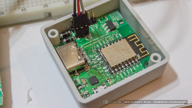
Well, at least the final testing concept board for this yet-to-be-name product line, again made right here in Silicon Valley, CA at RushPCB. This is a ESP-12e/ESP8266 carrier board, with some of the external logic to glue everything together. Most of parts I’ve been able to source from Arrow Electronics. They have free shipping on everything right now – no promo code needed.
Yes, giving Arrow a nice little plug, butter them up a little bit – as I will be applying for the Arrow & Indiegogo Get Certified program – because heck, I really could use some help (and money)! And well, they do seem to have slight better prices than other US distributors, and the Free Shipping kind of puts it over the top. But back to the board …
This Board Features
- ESP8266 via a ESP-12e
- ST LD1117 3.3v voltage regulator up to 15v VIN
- ESP8266 IO access via an HDMI connector
- FT231XQ Serial/UART to USB w/ USB connector
- For complete auto programing via esptool.py – solder jumpers to connect
- Serial RTS to ESP RESET
- Serial DTR to ESP GPIO0
- MOSFET VBUS or VSS auto Switch
- GPIO0, GPIO2 and RESET switches
- Needed 10k pull-ups via single 1206 Resistor array.
About the Modules
In additional to finally finding some enclosures, I’ve located a power supply, which is a Mean Well IRM-01 / IRM-02 / IRM-03. These are similar to the Hi-link HLK-PM01, however Mean Well parts are carried by a couple of the major US electronic distributors (unfortunately, not Arrow at this time), and though not a big deal right now – the Mean Well power supplies are also CE Marked. And in quality, these are pretty close in price to the China/India sourced Hi-Link modules.
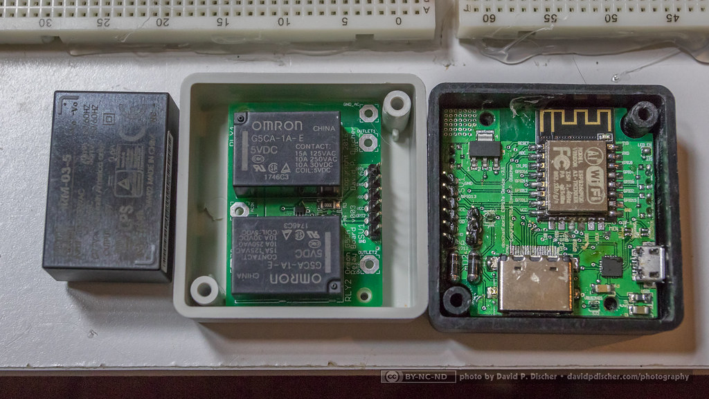
Some of the Enclosures
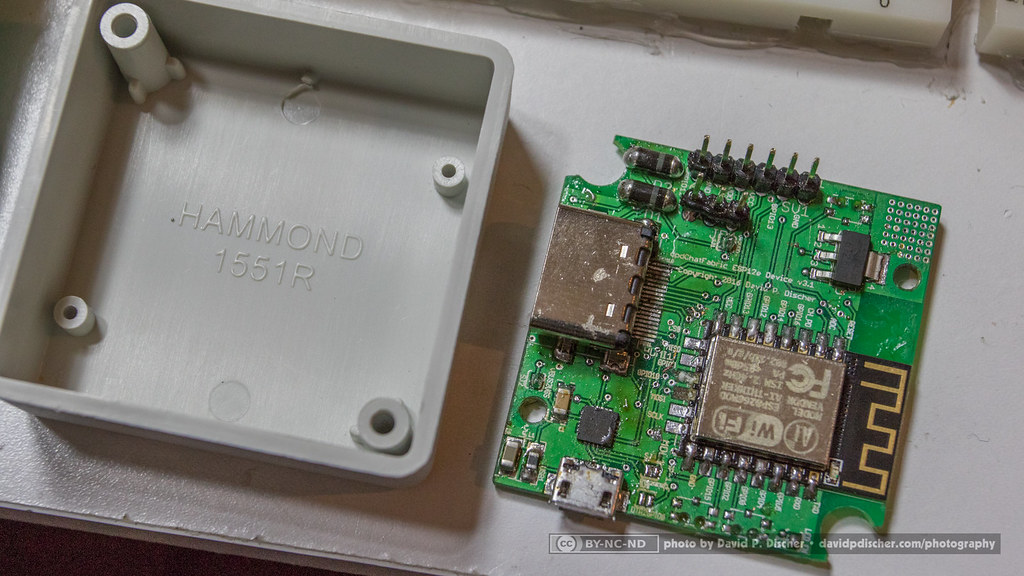
As I said in my previous post, for no good reason, I made it fit into a Hammond 1551R enclosure. Neat little trick, since the prototype services for PCBs don’t include cut-outs, I place some large holes at the edges, without copper or traces around them. It was pretty easy to cut the board. You can see it fits pretty well. The first product however will not likely be in this Hammond enclosure. There is a couple different Hammond enclosures I may use to contain the duplex outlets, however right now I’m leaning towards this Camden Boss enclosure. Though it feels a little thin and fragile. Looks brown, but technically sold as “gray”, but will likely source this enclosure in black.
What the … HDMI connector ?
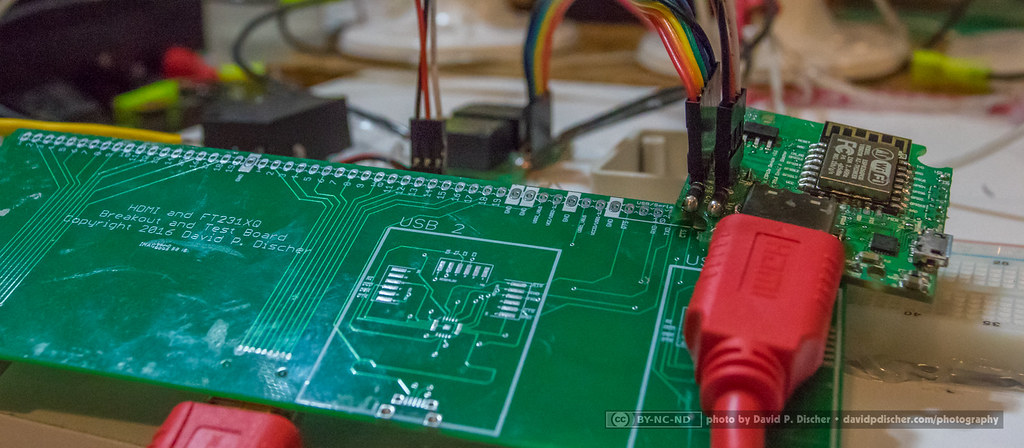
It’s not an HDMI port. I’m leveraging the connector as a low cost header/breakout cable. I needed something for board to board connections, especially durning development. (Unknown if it will stick around for the final product – I suspect that using an HDMI connector that is not for HDMI might trigger some licensing or other legal issues.) And HDMI connector takes up the same space as 6-pin 0.1″ breadboard headers, and gives 19 lines of IO. The 0.5 mm SMD pitch is pushing the limits for some prototype PCB services – so be aware if you use this on your designs. I like the idea of being to use commodity pre-made cables. Probably a good idea to use only passive cables. I could have picked a different cabling solution, and quite honestly wanted to use something like Molex’s Pico-Lock™ Connector System – but I couldn’t figure out what parts to order, how to get a cable, etc, etc. It’s not simply ordering a connector and cable like HDMI solution. RJ-45 was a consideration, but HDMI got me more lines for now. If anyone else has some connectors ideas for IoT interconnect – please let me know. Ideally, some of my products will just be the “smarts” and the sensors or relays will be connected via some sort of expansion connector. So think of a device in the 1551R enclosure, powered by a 5v USB phone charge via a micro USB port, and having some accessory ports – maybe connected via RJ-11 … run to window or door sensors, switches, temperate and humiditiy probes, relays, or other custom hardware. Kind of exciting. Modular and expandable IoT device hardware. Cool, huh? (yeah, it would involve “wires”.)
Mistakes in putting IO lines on the HDMI port
So, the ESP-12e has the lines to the SPI flash broken out on the board. If you change some of the setup to the flash, you can pick up a few extra GPIO lines. So I ran GPIO 9 and GPIO 10 lines out to the HDMI connector. However, every time I just connected an HDMI cable … with nothing else on the other side … I got massive amounts of garage over the serial port or flash read errors some or some sort of run-time exception. My guess is that putting these GPIOs over a big long wire acted like an antenna, putting enough noise on the IO lines to the flash, causing bit errors. So that teaches me. I wasn’t going to do it, but did it anyway. I lifted the pads off the board for GPIO lines, and it works fine now. I’ve corrected this already in v3.2. But I have nine more 3.1 boards … so I have some high temperature non-conductive tape on order, that will hopefully allow me to mask off these pads on the other boards.
Mistakes in the USB to Serial
Something to note, that I’ve found hard to find on the web and documentation, the FTDI Chip FT231X Transmit and Receive Lines do need to be crossed to your micro-controller. So connect TXD to RXD and RXD to TXD. However I got cute in the schematic layout – I tried to cross the TXD and RXD in the net names … see the image below :
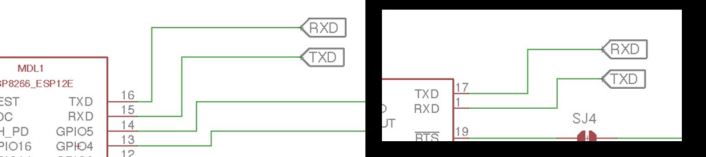

So, unfortunately this doesn’t work too well. I’ve “fixed” this for v3.2 of this board, but kept the lines into the HDMI connector on the same pins as the v3.1 PCB. I think I’m going to leave off the FT231X on this carrier board, so I don’t have to cut traces. Then use my HDMI and FT231X breakout board to program and test with. This way, both 3.1 and 3.2 boards (and future boards) will have the same pin outs on the HDMI connector. Enabling the creation of some sort of pseudo device docking station.
But before this, with squeezing things into 45mm x 45mm, I put some vias under the connector. This worked fine for the HDMI connector, but that had a plastic cover over the bottom of the connector. But with the USB connector, the metal shield came into contact with the D+ and D- lines of the USB bus via the vias. Oops. A little electrical tape let me work around it. Hopefully the high temperature tape will also help here.
Over Complicating things: MOSFET VBUS or VSS auto Switch
I bread boarded this design and seemed to work. Thought this would be a neat little feature. Something that could optionally be USB Bus powered, and seamlessly connect it to a different power source – while making sure to product against back currents into the USB Bus. The USB Bus power works perfectly via the P-Channel of the MOSFET. However, the N-Channel, with a 12-volt VSS, and even dropping R3 down to a jumper (0 Ohm) – the MOSFET is only ends up passing 10 – 10.5 volts … so 80% of input (before the diode). I understand the voltage drop over the diode, but I don’t understand why there is a voltage drop over the MOSFET. I haven’t actually tested with both power sources active. This was kind of the experimental piece of this whole board. I’m not sure when I’ll have a situation that I’ll need this for the actual product. Great for hobby and development boards, but for being embedded in a product, I don’t think its needed. Luckily, I have SJ1 – so I can bypass all this MOSFET crap. VDD is used to power for powering the relays.
Though I won’t be using this in future designs, it would be nice to understand this. I think a reference design using a MOSFET for an auto switching voltage source would be a useful little circuit. Oh yeah I’m using DMG1029SV-7 from Arrow and the datasheet is here. Part of me thinks this was just a poor choice of MOSFET.

Other Miscellaneous Things
Not shown on the pictures, but I do have some micro-miniature switches on GPIO0, GPIO2 and RESET lines. I had to order some more, because it turns out, these switches don’t hold up to my hot air reflow station really well – they were melted and were totally destroyed. Will have to be a bit more careful, and use the iron and not the hot air.
There are some LEDs in 0805 packages, and a 330 Ohm and 10k Ohm 1206-size resistor array on the board as well. I designed it with 10 pin, 8 resistor networks, but ordered 8pin, 4 individual resistors. I was actually able to make those works on the pads I had and how I had laid out the PCB. I’ve since order the correct part – or at least the part which is needed for the PCB – but haven’t yet assembled a board with them. It was a massive space saver – 1 x 1206 instead of 4x 1206 resistor.
The idea here is for the lights and switches is to use some light pipes and some, ugh, button rods so they can be seen and activated from outside the enclosure. Doubtful that my current layout will work in my enclosures, but it was yet another experiment to see how to achieve this.
Conclusions
Despite some major OPPSes on the layout of this board, I’m considering this a success. Maybe not an A, but a B or B+ at least. I’ll now be able to create some outlet enclosures, using parts and boards I’ve source entirely from US distributors(*), and PCB boards I’ve designed and created. So I’m on my way. I need to do a deep dive into software in October.
(*) OK, well, the ESP-12e is hard to source here in the USA. However, I’m setup with Espressif for direct purchase of the ESP8266 from China. Future designs will likely remove the ESP-12e, and have the ESP8266, SPI flash and crystal directly on my board. However, doing so will, for a consumer product, definitely require the device to go through FCC Part 15 testing. This is at least $10,000, and will not be feasible without funding. I can work around this by selling this as a “kit” or “hobbyist” product. This is based on the great research done by SparkFun on the FCC. At this, I’m filing this as a risk, and will cross that bridge when I get there.